

 Electronics
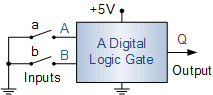
Also, sometimes we need an input to be present in it's default state and only need it to switch to the other state when the user enters the input (Pushbutton example). The circuit below seems like it achieves the purpose:
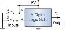
However, there are some problems. The problem with the first circuit is that when the switch is open, the input wire is neither HIGH nor LOW. Instead it is Floating between Vcc and Gnd. The problem with the second circuit is that when the input we want is logic LOW, the switch should be closed. This leads to shorting of the battery which can cause a lot of issues (From damaging the circuitry to energy losses). Hence, we need a different circuit to resolve these issues and that's where the concept of Pull Up/Down resistors was introduced.
Concept behind Pull Up/Down resistors:
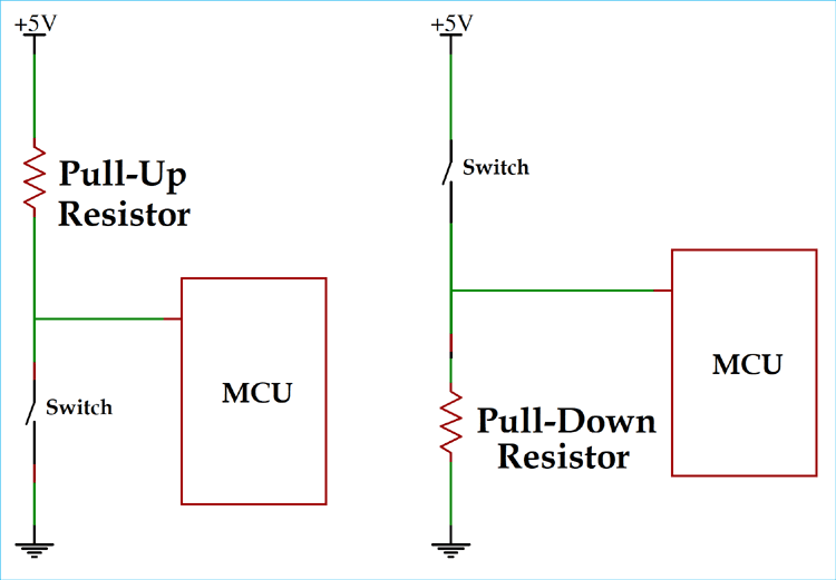
When a pull Up/Down resistor is used, the input terminal is automatically maintained at a valid default state. When the default state is logic HIGH, the resistor connects the input to Vcc and hence, known as Pull Up Resistor. If the default state is logic LOW, then the resistor connects input to Gnd and hence, known as Pull down resistor. They ensure that the input terminal is never floating and also won't allow shorting of the source. Now, that we understood the concept of Pull Up/Down resistors, the next step is to find what are their values. But before doing that, first we must understand the range of voltage for different digital states.
Logic levels
We know that inputs are nothing but electric voltages and hence they are continuous variables, i.e., they range over a continuum of real values (say from 0 to 5V). But we are trying to assign only two discrete valid states. Hence, there must be some mapping between the real voltage values and the discrete logic values. We can say that logic LOW is 0V (Gnd) and logic HIGH is Vcc (Usually 5V). However, practical systems need not have only either of these two voltages and can also have intermediate values like 4.3V or 1.7V. Hence, we need a range of values to be deemed as logic LOW and another range of values to be deemed as logic HIGH. The picture below illustrates one particular example (TTL 74LSxxx series of digital logic gates):
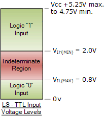
This image shows the valid logic levels and also the voltages which are neither LOW nor HIGH. In case of a floating wire, such voltages can occur causing a problem in the system. Once, the logic levels are known, we can find the Pull Up/Down resistor values using some quick math and understanding.
Finding the resistor values:
Pull up resistor value calculation:
Let's say that Vcc is 5V and the range of voltages that belong to the logic HIGH class is 3.0V to 5.0V. Also, let's say that the maximum current that flows from Vcc into the digital circuitry when the switch is left opened is 1.0 mA. There is no problem when the switch is closed as in that case, the input is proper logic LOW (0V). However, when the switch is open, the input wire is pulled up to Vcc using a resistor. Let its resistance be R_up (in ohm). Clearly, the maximum drop across it could be R_up mV (1 ma x R_up ohms). This drop is also equal to: Vcc - V_input Hence, V_input = Vcc-V_drop = 5-V_drop. Clearly, more the value of R_up, more will be the value of V_drop and hence, less will be the value of V_input. Hence, we need to choose R_up in such a way that V_drop doesn't reduce V_input below 3V for the max. current of 1mA. Hence: R_up = (5-3)/(1e-3) = 2 k ohms.
A more general formula is given below:

where:
- Vcc = Source voltage
- VIH(Min) = Minimum acceptable voltage for logic HIGH
- IIH = Maximum current through the pull up resistor when switch is open
Hence, R_up can have a max, of 2k ohm resistance but not more than that. Inface, it is advised to have a R_up below this max. value as that provides room for small error and noises in the voltage. However, having very low R_up can lead to huge currents leading to power losses and Joule's heating. Hence, optimum value must be chosen depending on the application.
Pull up resistor value connecting multiple inputs:
Let's assume a single pull up resistor is pulling up multiple inputs to Vcc. In that case, the resistance must be changed because now the total current through the resistor will be high. Say it is connected to 5 inputs and the max. current through all the inputs are 20mA. Clearly, the max. current through the resistor will be 5x20mA = 100mA. Hence, the new R_up value will be given by this formula:

This particular method of pulling up multiple inputs is called Fan-in of inputs. If the resistor pulls up 10 inputs then the fan-in ratio is 10.
Pull down resistor value calculation:
The concept is exactly same as that of the pull up resistor value calculation. The only changes are that now instead of having a minimum value for V_input, we will have a maximum value for it uptill which it can be deemed as a logic LOW. So, let's say the max. current in switch open state is IIL, the max. voltage is VIL(Max). Hence, the formula will be:
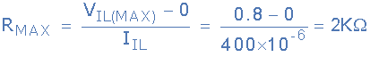
Again, the value of resistance we obtained is the maximum limit. It is advised to use a resistor with lower resistance for error tolerance. However, it can't be lowered as much as we want because that would lead to high currents. Hence, again we need to find the optimum value.
Pull down resistor value connecting multiple inputs:
The concept is exactly same as that of a pull up resistor connecting multiple inputs. You just need to find the max. value for R in a single-input case and divide that value by the fan-in ratio to obtain the new maximum limit.
Open-collector outputs and pull up resistor value calculation:
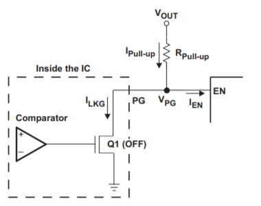
Sometimes, we may also need an output which is left open, i.e., it can either be logic LOW or must be left open so that the user can manually pull it up to a desired voltage level. Such circuits help in providing different voltage levels for the output terminal. For example, depending on the ratings of the load, the user may pull it up to a DC 5V source or a DC 25V source. The circuitry just acts as a control system and doesn't actually set the output HIGH. Such outputs are called as Open-collector outputs because usually they are the collector terminals of the transistors present within the internal circuitry. The diagrams are given below:
OFF case(Open circuit):
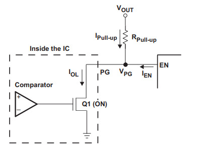
ON case(Closed circuit):
Now, let's find the limits for the Pull up resistance:
1. Maximum value: The max. value of the resistance is obtained in the OFF case. In this O case, theoretically, the transistor behaves like an open circuit. However, it'll still have some leakage current. The max. value of this leakage current will be given in the datasheet. Similarly, the max. value of the current throught the load will also be given in the datasheet. Hence, we can find the max. value of the pull up resistor current in OFF case. Now, the max. drop across the resistor would be this max. current times the resistance. This drop should be in such a way that the output terminal is having a voltage which is deemed as logic HIGH. Hence, the formula for R_up(Max.) is:
R_up(Max.) = (Vcc-VIH)/(I_pullup_OFF)
where:
- Vcc = Source voltage
- VIH(Min) = Minimum acceptable voltage for logic HIGH
- I_pullup_OFF = Maximum current through the pull up resistor when in OFF case
This limit is a maximum for the resistance as any other resistance higher than this value will increase the drop and can make the output voltage value go below the VIH(Min.) value.
2. Minimum value: The min. value of the resistance is obtained in the ON case. In this ON case, theoretically, the transistor behaves like a short circuit and hence, the output terminal is perfectly grounded. However, in reality, the transistor will have some resistance and hence, V_output will not be Gnd. Let the current through the transistor be I_L. The ratings for currents through the transistor and the load will be specified in the datasheet and hence, we can find the I_pullup_ON value based on those ratings. The formula for R_up(Min.) is:
R_up(Min.) = (Vcc-VIL)/(I_pullup_ON)
where:
- Vcc = Source voltage
- VIL(Max) = Maximum acceptable voltage for logic LOW
- I_pullup_ON = Maximum current through the pull up resistor when in ON case
This limit is a minimum for the resistance as any other resistance lower than this value will increase the I_L current leading to an output voltage more than the acceptable level for logic LOW.
References:
Refer these links for detailed explanation: